Silicon is the optical key that unlocks real-time, inline FTIR spectroscopy inside microreactors. It acts as the IR-transparent window through which you can continuously monitor chemical reactions—non-destructively and without disturbing the flow. This direct integration turns a standard microfluidic chip into a powerful, miniaturized chemical analysis laboratory.
Because silicon is inherently transparent to the mid-infrared radiation used in FTIR and is fully compatible with microfabrication processes, it becomes the foundational material for placing a spectroscopic probe directly over the reaction zone. This eliminates sampling delays and enables the precise, automated determination of reaction kinetics using only microliters of reagents.
Why Silicon is Uniquely Suited for FTIR Integration
The fundamental requirement for inline optical analysis is that the microreactor material does not absorb the probing light. Mid-infrared light (roughly 4000–800 cm⁻¹) directly excites the vibrational fingerprints of chemical bonds, making it ideal for identifying molecular structures and tracking concentration changes.
Silicon satisfies this requirement in a way few other microreactor materials can.
Unmatched Mid-IR Transparency
Silicon transmits IR radiation cleanly across the entire diagnostic region where most organic functional groups absorb.
It is essentially invisible to the very wavelengths you need to see your reaction. This transparency means that when silicon is used as a channel wall or a substrate, the FTIR beam passes through with minimal attenuation, delivering a high signal-to-noise spectrum directly from the reaction mixture.
Microfabrication Compatibility
Silicon isn’t just an optical material; it’s the workhorse of microfabrication.
You can etch microchannels, drill ports, and seal the chip with another IR-transparent silicon cover using well-established cleanroom techniques. This creates a monolithic, integrated device where the reactor and the optical window are the same piece of material, eliminating alignment issues and dead volumes.
From Substrate to Sensing Element: How Integration Works
Integrating FTIR into a silicon microreactor isn’t just about selecting a material; it’s about a deliberate design that places the spectroscopic beam directly into the flow path.
Capping Microchannels for Transmission FTIR
The simplest approach is to cap a silicon microchannel with another layer of silicon.
An incident IR beam traverses the stacked silicon windows and the fluidic channel, and the transmitted light is collected for analysis. This transmission-mode setup provides a direct measurement through the entire reaction zone, enabling real-time monitoring of chemical structures and species concentrations as soon as mixing occurs.
Microfabricated ATR Crystals for Problematic Solvents
Transmission mode struggles when the solvent itself absorbs too strongly.
Water, for example, completely blocks IR light in path lengths of more than a few micrometers. Here, the solution lies in an integrated silicon Attenuated Total Reflection (ATR) crystal. A silicon element is fabricated directly into the chip, creating an internal reflection where the evanescent wave probes only a micron-thick layer of fluid at the surface.
This overcomes the optical path-length limitation, making it possible to perform FTIR analysis on highly absorbing aqueous mixtures without dilution or sample extraction.
Optimizing Performance with Dielectric Coatings
Pure silicon is a good start, but its surface can limit performance in two ways: high reflectivity and potential chemical attack.
Applying a thin dielectric film transforms a basic silicon window into a rugged, high-transmission sensor.
Reducing Reflection Losses
Silicon has a high refractive index, which leads to significant reflection at each air-silicon interface.
This reflected light never reaches the detector, reducing your overall signal. A carefully deposited silicon oxide or silicon nitride layer (~500 nm thick) acts as an anti-reflection coating, minimizing these losses and boosting IR transmission through the assembled chip.
Enhancing Chemical Compatibility
The harsh chemical environment inside a microreactor can slowly etch or damage native silicon.
The same dielectric coatings provide a chemically inert barrier, protecting the optical surface and ensuring long-term measurement stability, especially when working with acidic or alkaline reactants.
Tackling the Challenge of Highly Absorbing Solvents
When water or similar solvents dominate the reaction, direct transmission becomes impossible.
The ATR Workaround with Silicon
The integrated silicon ATR element is not an add-on; it’s carved from the same substrate.
By directing the IR beam into this crystal and positioning the microchannel over its surface, you capture a spectrum from the immediate interface. The signal strength becomes independent of the channel depth, allowing you to quantitatively analyze reactions in water with the same ease as in organic solvents. This design keeps the entire analysis non-invasive and inline.
Understanding the Trade-offs and Pitfalls
Even a nearly perfect optical material has limitations. Relying on silicon without accounting for them can compromise your data.
The Wavelength Cut-off
Silicon’s IR transparency stops around 800 cm⁻¹ (below about 1250 nm). If your key functional groups absorb in the far-infrared region, silicon is not the right substrate.
You must verify that the vibrational bands you need to monitor lie within the 4000–800 cm⁻¹ window. Most organic reactions containing C-H, O-H, N-H, and C=O bonds are well-served, but metal-ligand vibrations or some lattice modes will be invisible.
Reflection Losses Without Coatings
An uncoated silicon window can lose over 30% of the incident IR intensity due to reflection at each surface.
For a transmission cell with two silicon pieces, this loss occurs four times, potentially degrading the signal below usable levels. Designing the system without an appropriate anti-reflection layer is a common and avoidable mistake.
Native Oxide Variability
Fresh silicon quickly forms a thin native oxide layer in air. While not as performant as a deposited coating, this uncontrolled film introduces variability in baseline transmission and chemical surface activity.
For reproducible quantitative work, a deposited, stabilized dielectric coating is far superior.
Making the Right Choice for Your Goal
Selecting the exact silicon integration approach depends entirely on what you need to achieve with your microreactor analysis.
- If your primary focus is rapid kinetic analysis of organic reactions: Cap your microchannels with an uncoated silicon window to get the simplest, most direct transmission measurement, but quantify your signal-to-noise budget first.
- If your primary focus is monitoring aqueous phase reactions or highly absorbing solvents: Integrate a microfabricated silicon ATR crystal directly into your chip to bypass path-length limitations completely.
- If your primary focus is long-term ruggedness and reproducibility: Always include a thin, deposited dielectric coating (silicon oxide or nitride) on your silicon windows to reduce reflection losses and shield against chemical attack.
Silicon’s unique combination of mid-IR transparency and microfab compatibility makes it the cornerstone of inline FTIR monitoring. By matching the integration method—transmission or ATR, coated or uncoated—to your specific reaction environment, you unlock the full potential of real-time, non-destructive chemical insight at the microscale.
Summary Table:
| Integration Method | Best Used For | Key Advantage |
|---|---|---|
| Transmission FTIR | Organic reactions & rapid kinetics | Direct measurement through the entire reaction zone |
| Integrated ATR | Aqueous phase & highly absorbing solvents | Bypasses optical path-length limits via evanescent waves |
| Coated Silicon | Harsh chemical environments & long-term testing | Reduces reflection loss and prevents chemical etching |
Elevate Your Chemical Engineering & Research Capabilities with LABPARK
Are you looking to implement advanced analytical processes and unit operations in your facility? LABPARK provides premium Educational and Vocational Unit Operations Pilot Plants across chemical engineering, bioprocess & biotech, and environmental & water treatment. We empower universities, research institutes, and enterprises worldwide with scalable, industrial-grade training and research systems.
Contact LABPARK today to discuss your pilot plant requirements and discover how we can customize a solution for your lab!
Related Products
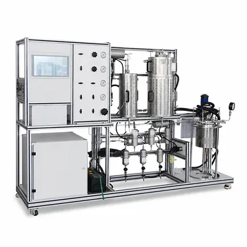
- Multi Functional Catalytic Reaction and Reactor Evaluation Educational Unit Operations Pilot Plant
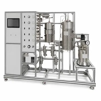
- Multi-Reactor Educational Pilot Plant for Reaction Engineering Unit Operations
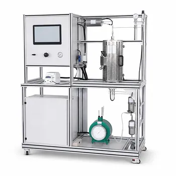
- Micro-Scale Gas-Solid Catalytic Reaction Educational Pilot Plant
- Educational Unit Operations Pilot Plant for Intraparticle Diffusion Effective Factor Measurement
- Tubular Reactor Flow Characteristics Determination Educational Unit Operations Pilot Plant
People Also Ask
- What reaction engineering principles are shown in a catalytic reactor pilot plant? SO2 Oxidation Guide
- Why is FTIR integration in catalytic pilot plants important? Real-Time Student Insights
- How to analyze active metal distribution & identify catalyst poisoning in pilot plants? Expert Diagnostic Guide
- How do temperature limits and WHSV influence catalytic reactor optimization? Scale-Up Guide
- Why is XPS Critical for Catalytic Reactor Pilot Plants? Optimize Catalyst Performance