The heart of your NIR analyzer’s performance lies in its photodiode detector material—a choice that directly dictates which chemical bonds you see and how much thermal engineering you need to see them clearly.
When selecting a photodiode for real-time monitoring in a chemical or bioprocess pilot plant, the detector material defines the usable wavelength range and directly determines whether thermoelectric (TE) cooling is essential. Silicon (Si) and Germanium (Ge) offer limited near-infrared coverage, while Indium Gallium Arsenide (InGaAs) stands out because its alloy composition can be tuned to extend from the visible to 2600 nm. However, accessing the longer wavelengths beyond ~1700 nm—where many overtone‑combination bands of organic molecules reside—narrows the band gap, amplifies thermal dark current, and forces the adoption of TE cooling to maintain a high signal‑to‑noise ratio.
The central insight: a standard InGaAs photodiode (53% In / 47% Ga) delivers high sensitivity at ambient temperature up to 1700 nm, covering most first‑ and second‑overtone bands. If your application demands the deeper molecular fingerprints between 1700 and 2600 nm, you must switch to a higher‑indium‑content graded‑lattice InGaAs detector and accept the cooling requirement needed to suppress thermal noise and preserve linearity.
The Detector Material Defines Your Spectral Window
Silicon and Germanium: Narrower Windows, Limited NIR Use
Silicon photodiodes respond only up to about 1100 nm.
This covers the transition region from the visible to the very early NIR, making them unsuitable for the rich 1200–2500 nm overtone‑combination bands that characterize organic functional groups.
Germanium extends the cutoff to approximately 1800 nm.
However, its sensitivity is often lower, and its thermal dark current can be problematic even at moderate NIR wavelengths, limiting utility in demanding real‑time process applications.
InGaAs: Tunable Band Gap for Broader Coverage
InGaAs is the workhorse of modern NIR process analyzers because its band gap can be engineered.
By varying the indium‑to‑gallium ratio, the detector’s spectral response is precisely matched to the analytical region of interest.
A lattice‑matched composition of 53% In / 47% Ga, grown on an InP substrate, yields a cutoff wavelength near 1700 nm.
This standard InGaAs photodiode exhibits high specific detectivity (D*) and operates with excellent sensitivity at ambient temperature, simplifying the analyzer design.
When the alloy is shifted to higher indium content (e.g., 82% In / 18% Ga) through a graded lattice structure, the cutoff extends to 2600 nm.
This region is critical for real‑time monitoring of complex feedstocks—such as fermentation broths or hydrocarbon streams—where the combination bands provide unique molecular specificity.
The Cooling Threshold: Why Longer Wavelengths Demand Thermal Management
The trade‑off for the extended wavelength coverage is a narrower band gap.
A smaller band gap generates substantially more thermal dark current, which degrades the signal‑to‑noise ratio and makes sensitive measurements difficult without cooling.
Therefore, high‑indium‑content InGaAs detectors require thermoelectric (TE) cooling.
Cooling stabilizes the detector temperature, suppresses dark current, and restores the linearity and detectivity needed for quantitative process analytics.
Matching Detector Characteristics to Pilot‑Plant Dynamics
Speed, Linearity, and Sensitivity: Why InGaAs Photodiodes Excel
In a pilot plant, chemical concentrations or bioprocess parameters can change rapidly.
The detector must capture these dynamics without lag or distortion.
InGaAs photodiodes offer high linearity, fast response times, and excellent sensitivity.
Compared to photoconductive detectors like lead sulfide (PbS) or lead selenide (PbSe)—which suffer from saturation, poor linearity, and limited speed—InGaAs photodiodes deliver the real‑time fidelity required for process analytical technology (PAT).
Thermal Noise and Signal‑to‑Noise Ratio
Detector performance is ultimately limited by noise.
For ambient‑temperature standard InGaAs, shot noise and Johnson noise remain low enough to achieve robust measurements in the 900–1700 nm range.
When you push into the 1700–2600 nm window with a graded‑lattice InGaAs detector, thermal dark current becomes the dominant noise source.
Without TE cooling, the elevated dark current erodes sensitivity and can introduce drift, compromising the reproducibility of critical quality attributes.
Active cooling not only reduces dark current but also stabilizes the detector’s spectral response over time, a key requirement for chemometric models that rely on consistent spectral baselines.
Understanding the Trade‑offs
Choosing the right detector is never a one‑size‑fits‑all decision.
The ambient‑temperature standard InGaAs photodiode offers simplicity, lower cost, and robust performance for many common NIR methods—but it only reaches 1700 nm.
Extending coverage to 2600 nm brings the ability to probe deeper into the molecular fingerprint region, enabling analysis of more complex samples or lower‑abundance components.
The cost is higher complexity: a thermoelectrically cooled housing, additional power supply, and potentially a longer warm‑up time.
There is also the risk of over‑engineering.
If your process can be fully characterized with the bands below 1700 nm, adding cooling yields no significant analytical benefit and introduces unnecessary maintenance overhead.
Additionally, while non‑photodiode detectors like PbS might seem attractive for their low cost and wide spectral range, their non‑linearity and slow response often make them unsuitable for dynamic pilot‑plant environments where real‑time control actions depend on linear, high‑speed data.
Making the Right Choice for Your Pilot‑Plant Goal
Your final selection should align with the molecular information you truly need, the speed of your process, and the environment in which the analyzer will operate.
- If your primary focus is rapid, multi‑component monitoring of standard organic feedstocks in transparent liquids (e.g., solvent blends, clear reaction mixtures): Choose a standard ambient‑temperature InGaAs photodiode optimized for the 900–1700 nm range to get high linearity and low‑maintenance operation.
- If your primary focus is analyzing complex bioprocess streams, solids, or samples where crucial combination bands appear beyond 1700 nm (e.g., fermentation monitoring, protein‑rich slurries, moisture in powder blends): Invest in a graded‑lattice InGaAs detector with TE cooling to secure the extension to 2600 nm while suppressing thermal noise.
- If your primary focus is on a permanent installation where speed is not critical and you require only occasional spectra from a scanning monochromator: Photoconductive PbS/PbSe detectors may be considered, but be prepared for non‑linearity and slower acquisition that can limit real‑time control in a pilot plant.
- If your primary focus is balancing performance with cost and the bulk of your target analytes absorb below 1700 nm: Stay with the uncooled InGaAs and use multivariate models that can compensate for any minor matrix interference without the need for the longer‑wavelength combination bands.
The photodiode detector material is the gateway to your process’s molecular story; selecting the right one ensures you capture every critical detail with the clarity and speed a pilot plant demands.
Summary Table:
| Detector Material | Wavelength Range | TE Cooling Req. | Ideal Application & Characteristics |
|---|---|---|---|
| Silicon (Si) | Up to 1100 nm | No | Early NIR/Visible range; limited organic band detection |
| Germanium (Ge) | Up to 1800 nm | Optional / Recommended | Limited sensitivity; high thermal dark current |
| Standard InGaAs | 900–1700 nm | No | Standard organic feedstocks; high linearity and speed |
| Extended InGaAs | 1700–2600 nm | Yes (Critical) | Complex bioprocesses, solids; suppresses dark current |
| PbS / PbSe | Up to 3000+ nm | Typically Yes | Non-linear and slow; not ideal for dynamic real-time control |
Optimize Your Process Monitoring with LABPARK
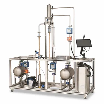
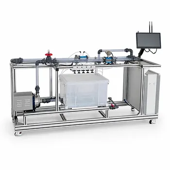
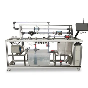
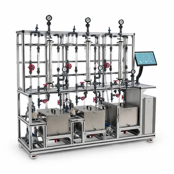
Are you looking to integrate advanced real-time monitoring into your pilot scale operations? LABPARK provides premium Educational and Vocational Unit Operations Pilot Plants in chemical engineering, bioprocess & biotech, and environmental & water treatment. Designed specifically for universities, research institutes, and enterprises, our pilot plants enable precise process analytical technology (PAT) integration to ensure reliable data and hands-on operational excellence.
Let us help you select the right instrumentation and systems for your chemical and bioprocess goals. Contact LABPARK today to discuss your custom pilot plant requirements!
Related Products
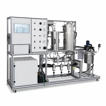
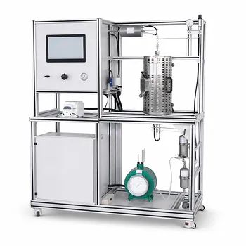
- Multi Functional Catalytic Reaction and Reactor Evaluation Educational Unit Operations Pilot Plant
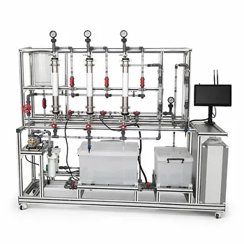
- Multifunctional Membrane Separation Educational Pilot Plant with Ultrafiltration, Nanofiltration, Reverse Osmosis
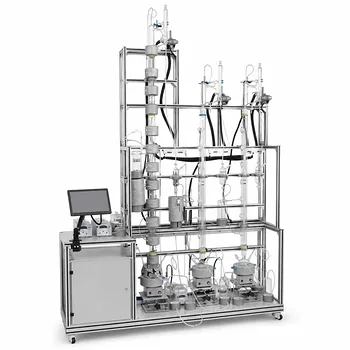
- Continuous Batch Extractive Distillation Educational Pilot Plant
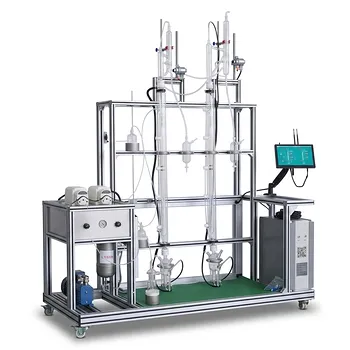
- Multi-Functional Special Distillation Educational Pilot Plant
- Rising and Falling Film Evaporation Educational Unit Operations Pilot Plant
People Also Ask
- What reaction engineering principles are shown in a catalytic reactor pilot plant? SO2 Oxidation Guide
- How does feed gas flow rate affect catalytic RFR yields? Optimize Pilot Plant Performance
- Why is FTIR integration in catalytic pilot plants important? Real-Time Student Insights
- How to analyze active metal distribution & identify catalyst poisoning in pilot plants? Expert Diagnostic Guide
- How to study catalyst poisoning & regeneration? Master catalytic reaction life cycles.